Scanning Electron Microscope
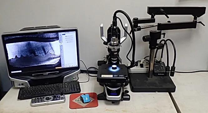
Scanning Electron Microscope
Secondary Electron Imaging (SEI):
Secondary Electron Imaging creates a high-resolution, high depth-of-field image and gives excellent surface definition of the sample. This is good for imaging purposes to see fracture surfaces, surface features, particle sizes, porosity, or lack of fusion.
Backscatter Electron Imaging (BEI):
Backscatter Electrons give data about the different elements that may be scattered in a sample. The grayscale of the image will change depending upon the atomic wait of the target. This allows for identification of materials within a sample that may not be homogeneous.
Energy Dispersive Spectroscopy (EDS):
Our scanning electron microscope is equipped with a silicon drift detector (SDD) EDS. This equipment identifies what elements are present within a sample and to what percentage they are present. This is helpful in the identification of materials as well as the presences of contaminates. Our SEM operator’s have three years of experience in scanning electron microscopy.
Sample Preparation:
The highest resolution imaging available within the Scanning electron Microscope requires an electrically conductive sample. If a sample can not conduct electricity, it will hold an electric charge when bombarded with electrons by the microscope. A charged sample prevents detailed imaging. To prevent this problem, we offer a palladium sputter coat to coat non-conductive samples with a microscopically thin layer of palladium. This layer dissipates any charge produced by the electron microscope and allows for complete high-resolution imaging. Because palladium is rarely found in samples, it can be ignored during elemental analysis.
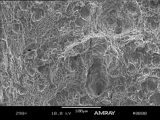
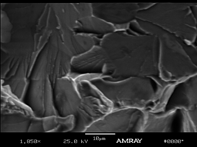
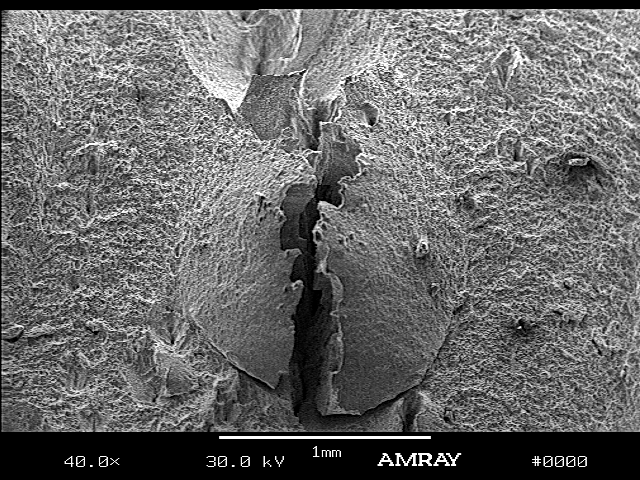
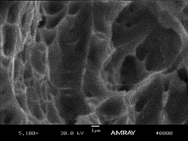
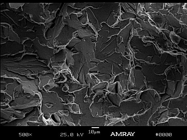
Secondary Electron Imaging photos are shown above from different sample such as carbon steel, stainless steel, and aluminum. These photos where taken at different magnification ranging from 40X – 5,100X.
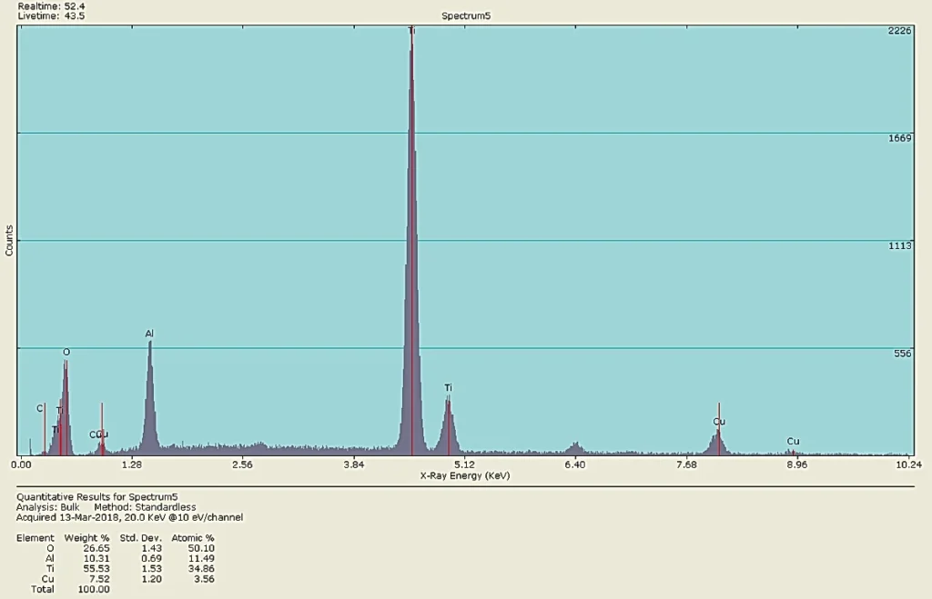
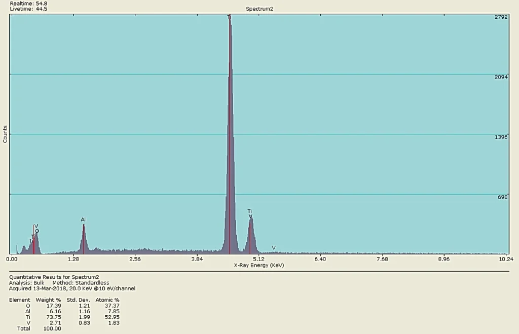
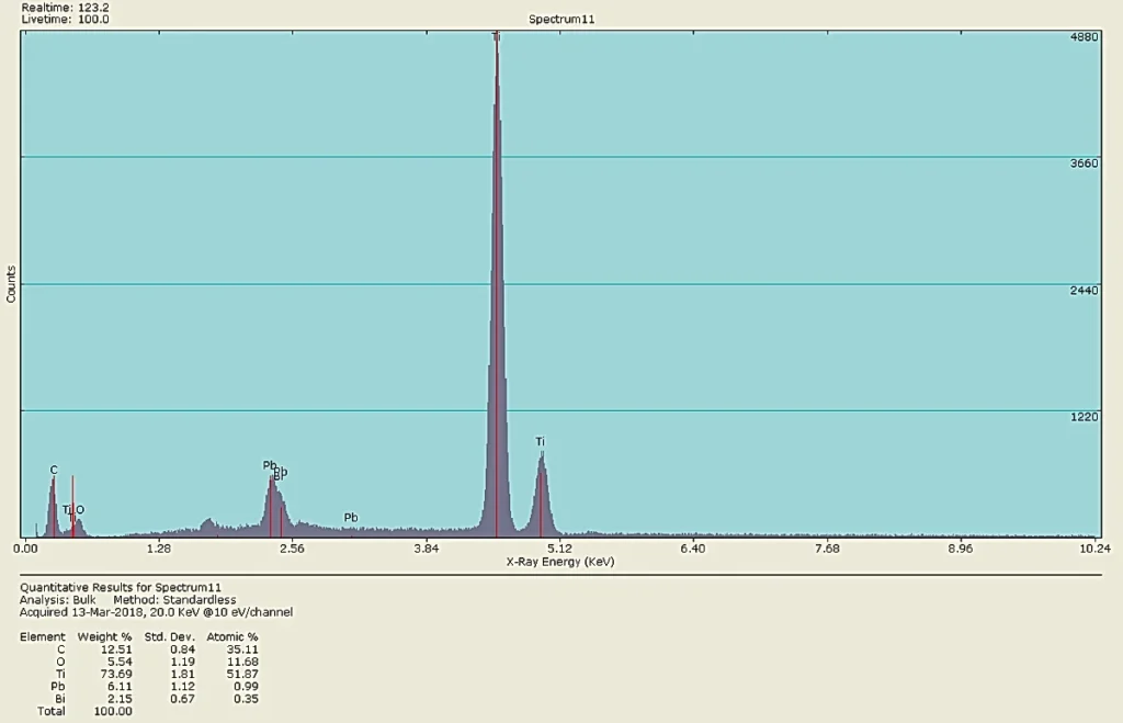
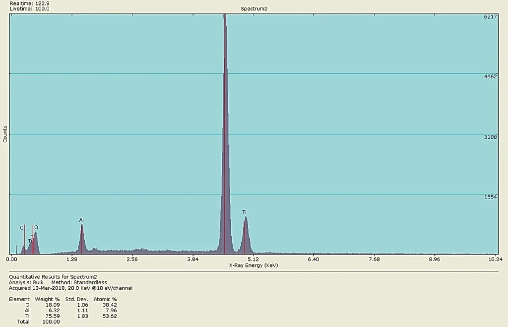
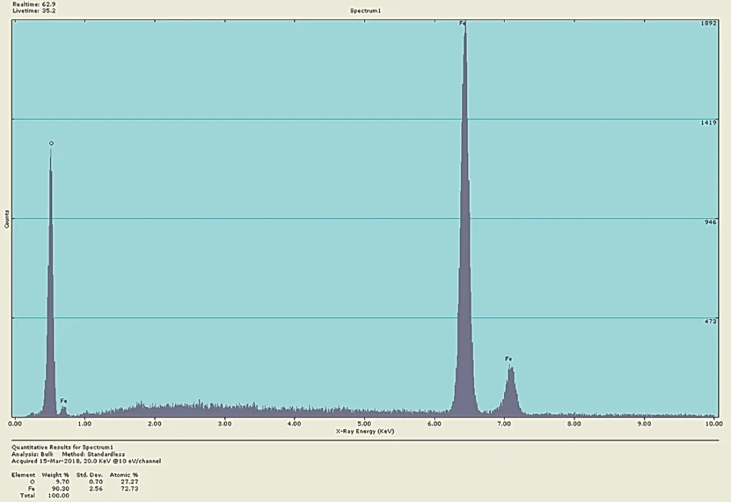
Energy Dispersive Spectroscopy photos are shown above from different sample such as carbon steel and titanium.
